
I was at a compound semiconductor conference early this year where they were hopeful that compound semiconductors might soon become part of the silicon industry, a great hope for many years, but I was thinking, no, it has already happened. You guys missed the industry shift. It’s already happened and you’re totally unaware.
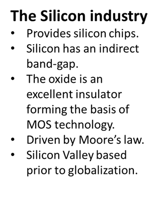
The old semiconductor space was actually two almost completely separate areas for decades. There was the old Silicon Valley stuff based very heavily on silicon, and based very heavily in Silicon Valley until globalization outsourced it to Asian areas, such as Taiwan, China, Singapore, Malaysia and elsewhere.
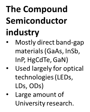
Then there was the compound semiconductor area. Totally different, based on Telecoms, like AT&T, British Telecom and others, some hi-tech companies like Phillips and then, of course, the Universities. There was no central hub like Silicon Valley was for the silicon people, but it had many centres of excellence all over the developed world.
I was brought up as a young PhD in the compound semiconductor world. Part of the reason universities were heavily involved in that area is because it is a research rich space where lots of publications can be had. Of course, research happens in the silicon world too, but it’s largely in-house company-based research, which doesn’t necessarily see the light of day for many years, not as good an environment for publishing and getting a PhD.
For both the silicon and compound semiconductor spaces there were setbacks and major advances. I remember those of the compound semiconductor area best. The diagram below provides a broad overview. One of the biggest breakthroughs in the 1990s was the development of GaN based blue LEDs, this led to a multi-billion dollar industry, room lighting and a research rush, which was good because a couple of years later there was a break through at AT&T Bell in software engineering that sped up data transmission to the point where most of the Telecoms around the world decided they didn’t need to do compound semiconductor research any more. Many of those researchers from the Telecoms were let go but moved to nitride research in Universities.
Now move forward to 2002-2003 when the dot.com collapse occurred, it was basically a boom based on compound semiconductors used for optical transmission, newer companies like JD Uniphase and Nortel boomed for a while, software advances were limited at this stage so that compound semiconductors were needed again, but oversupply and overpromise created a bubble that burst. Then in 2007-2008 the Global Economic Collapse occurred, investors had already become more conservative because of the dot.com collapse but investment dried up after the Global Collapse (I’m totally ignoring the solar cell bubble, that’s a separate economic disaster related to over-investment, a separate area of semiconductors entirely). But here is where things get interesting, the recovery from 2008 was so long that governments also pealed back on scientific grants for many, many years. Compound semiconductor research was based on MOCVD and MBE systems worth close to a million (or several hundred thousand) dollars or more. Soon, after 2008, Aixtron and Veeco stopped offering systems of that size for MOCVD research because no one could afford them, MBE system providers struggled. A whole generation of PhD’s brought up on MOCVD and MBE film growth systems for compound semiconductors couldn’t get grants for those systems when they started their own groups, however atomic layer deposition (ALD) systems could do compound semiconductors and were very much more affordable, grants were available to buy those.
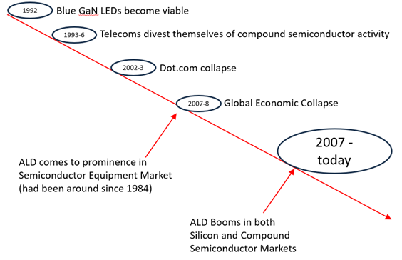
As it happened, around then the silicon part of the industry started to need ALD systems. A Berenberg Equity Research, Semiconductor Equipment Study (22/Jul/2013) placed the 2008 ALD systems part of the film equipment deposition market at maybe 1% of the total market, but by 2012 it was closer to 8% of the market. In 2013 the ALD equipment market was US$480 million. The market had a CAGR (compound annual growth rate) of 8.0%. In 2023 it’s been estimated that the ALD equipment market was worth US$3.9 Billion and the CAGR was 10%. (https://www.marketsandmarkets.com/Market-Reports/atomic-layer-deposition-ald-equipment-market-96683066.html). The reason for all this change was driven by Moore’s law, dimensions in silicon became smaller so that only ALD could deliver the layers of interest, and those layers were made of newer materials. Compound semiconductor materials, like TiN, HfN, AlN, dozens of others. The silicon industry now routinely uses compound semiconductors, but deposited by ALD, not a new method, but one that snuck up on the old MOCVD and MBE system users. The main annual ALD conference can attract over 1000 participants, making it one of the biggest compound semiconductor venues in the world and it regularly attracts silicon based participants from Applied Materials, Lam Research and other billion per quarter turnover companies from the silicon part of the industry. My message to the rest of the compound semiconductor community, still largely MOCVD and MBE based, using the old equipment still there in universities is, sorry dudes, compound semiconductors are already an integral part of the silicon industry, you just missed it. Maybe think about augmenting your research with some related to ALD.